Tel:0371-55983628

邮箱:sinomach-dia@diamondgroup.cn

tel:0371-55983628

邮箱:sinomach-dia@diamondgroup.cn

logo
English
Home
About Us
Products
Applications
Technological Innovation
News Center
Contact Us
Products
Applications
English

Tel:0371-55983628

邮箱:sinomach-dia@diamondgroup.cn

tel:0371-55983628

邮箱:sinomach-dia@diamondgroup.cn

Etching Tray.jpg
Etching Tray.jpg
Etching Tray

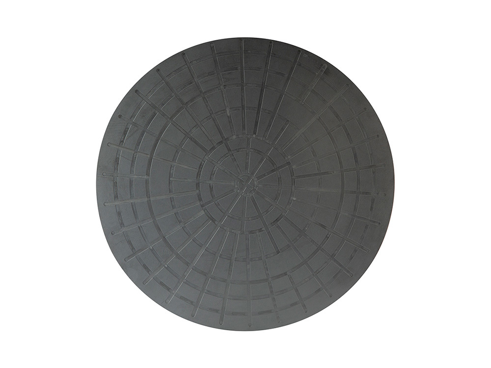
Mainly used for ICP etching process of epitaxial thin film materials (GaN, SiO2, etc.) for LED wafer chips, precision ceramic parts for semiconductor diffusion, and MOCVD epitaxial process for semiconductor wafers.

Adopting high-purity pressureless sintered silicon carbide ceramic material, it has the characteristics of high hardness, corrosion resistance, wear resistance, long service life, etc., and the product has high precision and good etching uniformity of the wafer epitaxial layer. Diameter range: 50~500mm, tray thickness: 3~20mm, can design and manufacture various non-standard products.

0371-55983628
sinomach-dia@diamondgroup.cn
Contact Us
SINOMACH-DIA WEBSITE GROUP
Copyright©Sinomach Diamond (Henan) Co., Ltd. All rights reserved
豫ICP备2024064511号-1
Copyright©Sinomach Diamond (Henan) Co., Ltd. All rights reserved
豫ICP备2024064511号-1