
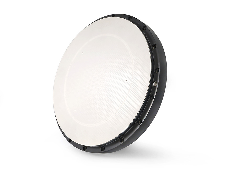
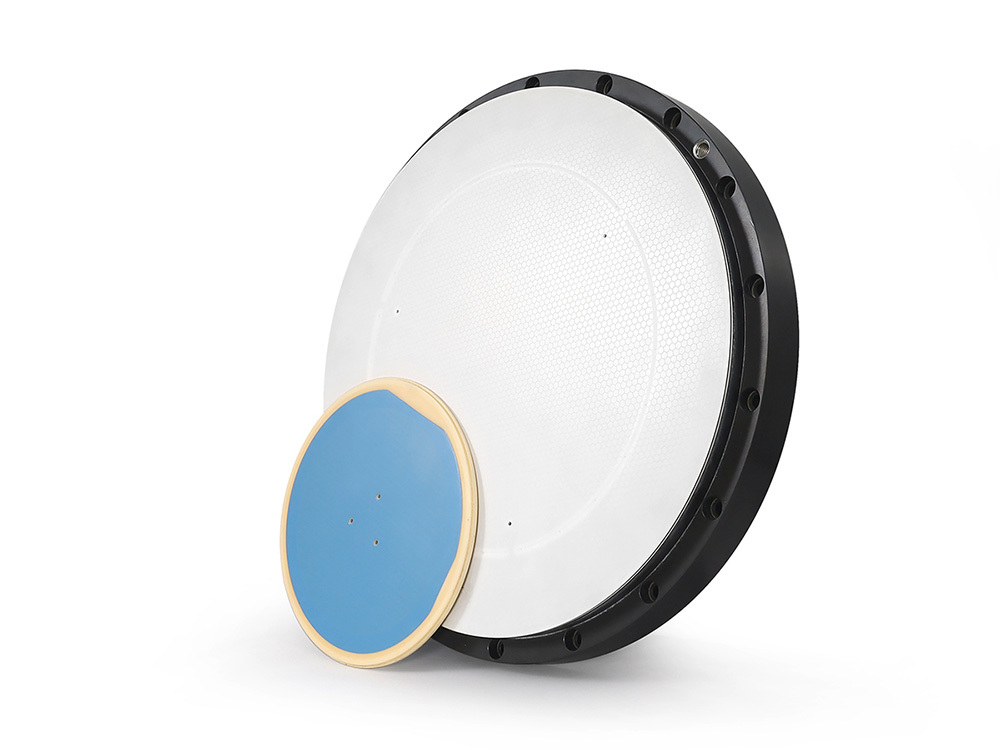
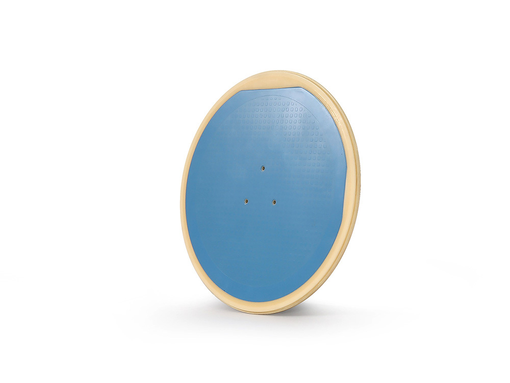
Mainly used for core key processes such as etching, thin film deposition, ion implantation, ashing, etc. in semiconductor front processing.
Adopting the principle of electrostatic adsorption for flat and uniform clamping of ultra-thin clean wafers, it has the characteristics of uniform adsorption force, no pollution, no damage, and can be applied in high vacuum environments.
The material is alumina ceramic (Coulomb type, purity 96%, 99.6%), which can provide products of 12 inches and below, with a working temperature of -30 to +180 ℃; Ceramic surfaces can be slotted, embossed, and have optional roughness.